Laser Engineered Net Shaping (LENS) is an Additive Manufacturing (AM) technology where powdered material is fed into a laser-induced melt pool and solidified in layers. Metal/alloy LENS processing is explored in this project.
 Fig.1. LENS deposition schematic.
The schematic shows a stationary deposition nozzle resting above a moving substrate. Using a high power focused laser beam the deposition nozzle creates a melt pool on the substrate surface, and immediately delivers powdered material into the area via a tight dry powder stream. The meltpool forms on the axis of the deposition nozzle, and as the substrate moves the molten regions and the added powder solidify into a deposit.
The process is versatile and industry-friendly due to a unique set of capabilities including full density deposit, multi-material and functionally graded part fabrication, large (meter scale) working areas, and curved surface processing. Harnessing these capabilities to deposit steels, titanium alloys, and superalloys LENS processing can be used for freeform fabrication as well as component repair lending it applications in aerospace, power transmission, heavy industry, etc.
The LENS deposit has a microstructure that is distinct from the substrate. Fig.2 shows an experimental EBSD plot of the deposit microstructure as a representative image.
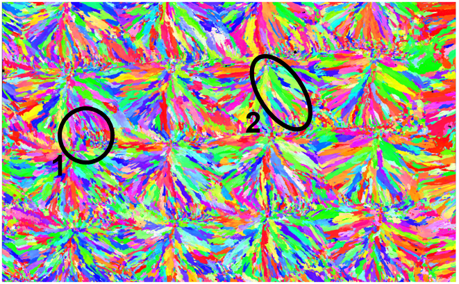 Fig.2. EBSD plot of LENS microstructure out of plane of meltpool propagation.
The image shows a large disparity between grain sizes as well as regions of more defined grain axis orientation (Fig.2.2) and regions os small and more equiaxed grains(Fig.2.1). Furthermore an altogether different microstructure is observed in the in plane EBSD plot (Fig.3) indicating anisotropy of the deposit with respect to scanning geometry.
 Fig.3. EBSD plot of LENS microstructure in plane of meltpool propagation.
This project draws its data from simulation of the LENS-type process which generated 3D micristructures as a function of an array of processing parameters Fig.4. From these the microstructure features such as relative grain size, directionality, and orientation are to be studied. The similarities and differences between the simulated data setes and the experimental EBSD plots can also be investigated in this work.
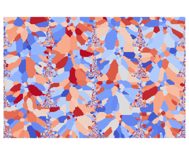 Fig.4. SPPARKS simulated microstructure resulting from LENS-type processing.
References
[1]http://www.intechopen.com/books/titanium-alloys-towards-achieving-enhanced-properties-for-diversified-pplications/numerical-modeling-of-the-additive-manufacturing-am-processes-of-titanium-alloys
[2] http://www.lpwtechnology.com/technical-information/laser-metal-deposition/
[3]http://www.3ders.org/articles/20130612-optomec-launches-new-3d-printer-for-metal-additive-manufacturing.html
[4]”AM-MicrostructureWIthParameterVariationCompressed” T. Rodgers Sept. 14th 2015